
The AI/DI universal inputs on the CFox and RFox modules (this does not apply to DI modules C (R)-HM-1113M and C(R)-HM-1121M), which will be used as D1 digital inputs (designed as inputs for potential-free contacts) need for a proper assessment of the switching
(sometimes referred to as the log. 1) to keep a maximum voltage at their own input. In other words, the maximum values of the input resistance of the input circuit have to be observed, and analogically, after opening the input (log. 0) it is necessary to comply with the minimum necessary voltage on the input, or the minimum input resistance.
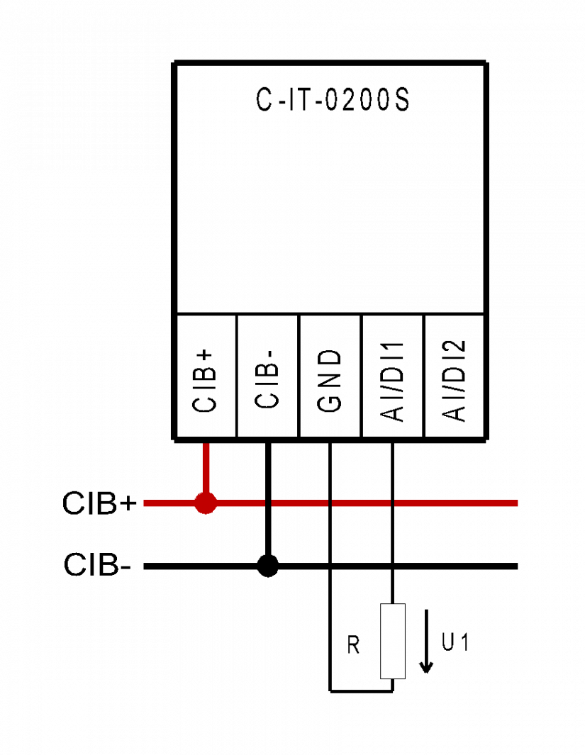
Fig. 1. The binary input circuit – measuring the parameters
Notes:
-
The module in the figure is C-IT-0200S. The same connection applies to all modules that have the DI inputs switched against the ground terminal GND, i.e. it does not apply to the DI of the modules C(R)-HM-1113M and C(R)-HM-1121M.
|
Input DI: |
The voltage U1 on the input |
The resistance R of the Input circuit |
|
Switched (log. 1) |
< 0.6 V |
< 0.5 kΩ |
|
Open (log. 0) |
> 1.3 V |
> 1.5 kΩ |